Introducción
この金曜日の夜は長く待ちわびていた瞬間です。任天堂がついに、ゼルダの伝説から始まる…新しいゲーム機、Nintendo Switchを発売したのです。さあ、ひとまずゲームのことは忘れて、早速ハードウェアの中身を見てみましょう。ここではiFixitに全てを任せて、iFixitのツールたちを自由に探検させてください。私たちと一緒に分解ショーを楽しみましょう!
ゲームは他の誰かに遊んでもらい、FacebookやInstagramやTwitter 、Twitter 日本語版 をフォローして新しい情報を見つけてください!
Qué necesitas
Resumen del Video
-
-
皆さん、メリースイッチマス‼︎ 任天堂の新しいハイブリッドの携帯式ゲーム機がどんなハードウェアを揃えているのか見てみましょう。
-
NVIDIA社製 カスタマイズされたTegraプロセッサー
-
静電容量方式タッチスクリーン 6.2インチ、1280×720ピクセル出力解像度(HDMIケーブル経由で1920×1080ピクセル)
-
32GB(microSDHCかmicroSDXCメモリーカードは最大2TBまで認識可能)
-
規格802.11 a/b/g/n/ac Wi-Fi, Bluetoothバージョン4.1、USB Type-C端子の充電ポート、3.5 mm オーディオジャックーSwitchドックへの接続や本体の充電に使用
-
ステレオスピーカー
-
充電可能なリチウムイオンバッテリーバッテリー持続時間 約2.5~6.5時間
-
取り外しが可能なワイヤレス式Joy-Con コントローラー
-
-
-
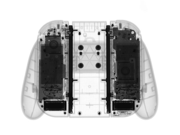
分解作業はとてつもなく困難です。私たちの親友であるCreative Electronは筐体全体をレントゲン撮影してみれば、何かの助けとなると考えました。
-
この画像を見ているるとハードウェアの詳細を早く見たいという思いに駆られます。外箱から本体とドックを取り出して、さらにレントゲン撮影をしてみました。
-
レントゲン写真は置いておいて、早速分解用のツールを取り出しましょう!
propaganda? where?
They spy, we spy but we won't tapp that...
A beefy battery? Where? *Laugh track*
-
-
-
まず最初に任天堂のお供え物の品々を広げてみましょう。コンソール、2セットのJoy-Con、ドックとJoy-Conグリップがあります。
-
本体に接続されたJoy-Conを本体に接続すると、Switch コンソールは横幅約9.4インチ、縦の長さは4インチで、奥行きはわずか1.5インチです。
-
Joy-Conのコンソール機能が加わったにもかかわらず、重量はわずか約399gです。これは 約499gのWii U GamePadと比べて、軽量化されました。
-
-
-
さあこの分解をギア全開にスイッチしましょう!
-
最初に注目するのは(変なドミノのロゴではなく)モデル番号~HAC-001です。
-
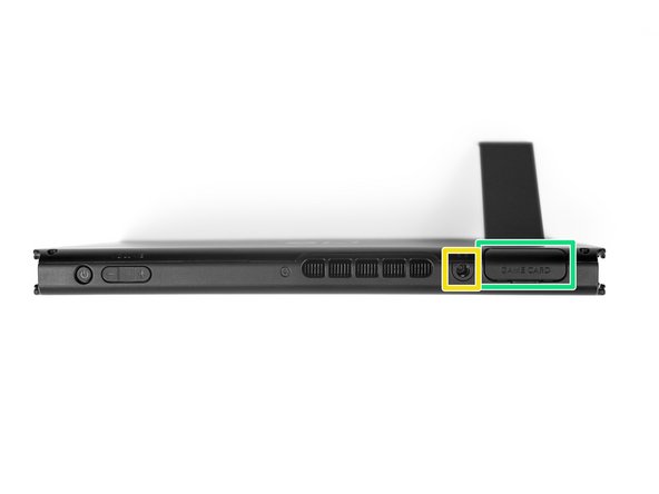
裏側に回ってみるとポートが確認できます。
-
microSDメモリーカードは(とてつもなく堅い)キックスタンドの底にあります
-
USB Type-C端子(ドック用)
-
標準3.5 mmヘッドホンジャック
-
任天堂ゲームカードスロット
Any chance the USB-C port supports Thunderbolt 3? I've been holding out hope it does and Nintendo will sell a "Pro Dock" that has an eGPU for better performance while docked.
You could do that with USB 3.1..
3.5mm headphone jack. You didn't mention anything about TRRS. Does that mean that there is no audio / microphone in?
-
-
-
残念なことに、トライポイントネジがSwitchの入り口を守衛しています。しかし、私たちは持てるMako Driver Kit - 64 Precision Bitsのうちの1つを使えば良いのです。
-
ここにトライポイントネジがあるということは、任天堂が’侵入禁止”のサインを出していると言えます。しかし私たちはもう通過してバックカバーを簡単に持ち上げましたーネジを外せばクリップや接着剤はありません。
-
フタを開けてみても現れるのはー特にありません。ただのメタル製シールドです。
-
しかしながら、ケースに入っていないモジュラー式microSD カードは簡単に取り外せます。これはストーレッジの容量を増やす際にはとても良いニュースです!
Whats the model of SD card reader will it read UHS 3 SD cards??
2mm Tri-Wing screws.
OK, This is extremely misleading. Good thing I’m a repair tech. There are also about 5 more phillips screws around that need to be removed before the back will come off. One by the SD card reader, one on each side in the center, 2 on the bottom and one on the top
Hi Jonathan, this is just a teardown, and as such we skip some disassembly steps to get to the more interesting stuff quicker. It’s not meant to be used as a repair guide. We do have more more in-depth guides here that can be referenced for repairs.
For some reason my screws were different in my switch I was trying to repair. I ordered the screwdriver that came with 2 bits and the se card reader but the bits wouldn’t fit the screws.
There are more screws than this guide will say.
1x middle of each joy-con rail (2 total).
2x bottom near the charge port
1x top near the audio jack
1x just under the microSD flap
each is a small Phillips head.
Hi! Sorry for the confusion with screws! This is a teardown! There is a warning at the top but it might have been missed: “This teardown is not a repair guide. To repair your Nintendo Switch, use our service manual.”
The platic thread of one of the screws broke while screwing it out.. I used to push the screw a little bit to prevent over-turning the head while unscrewing - it broke while pushing. Maybe it was a bad assembly, but its worth mentioning that it can possibly break inside.. and you have to deal with a loose screw after then. (Any Ideas?)
How can you to a teardown guide, without showing witch screws to remove, i thought you ifixit guys knew your stuf and were indebth, will find another guide screw this
Yeah I'm attempting something that requires complete disassembly, it would be nice to have a generic guide for that that includes all the steps rather than having to look up how to remove each individual component. I thought the teardown would be the obvious place for that, but apparently this is just, what, for entertainment purposes? Idk, I think it's definitely possible to show all the interesting internals while giving a detailed step-by-step guide for total disassembly, especially for guys like me who mainly just need to know where the screws are.
-
-
-
そしてついに私たちが待ち望んできた瞬間が来ました。内部を開いてみます。ついにありました!
-
それは…まるでコンピューターのようです!バッテリー、ヒートパイプ、放熱グリス、ファン。全て揃っています。
-
紫色の小さな塊をみてみると、このメタル製のプレートは構造上のサポート以上の役割があります。熱をヒートパイプからリアケースに運ぶヒートシンクです。
i don’t think it would hurt to do so, but i am no expert.
is the battery a single or multi-cell unit?
-
-
-
安全第一をモットーに、バッテリーコネクターの吸盤から接着剤を剥がす前に、バッテリーコネクターを外します。
-
Switchのバッテリーは16 Wh で、Wii U GamePadの交換可能バッテリー5.6 Whに比べると容量アップしてます。ですが、これはSwitchを動かすもので、飾りではありません。
It is user replaceable, but it was meant to cause replacement difficulty, which discourages inexperienced repairers.
It means is not that easy, you have to tear it down almost completely in order to replace it.
whats the weight of the switch battery in grams? and what type of battery cell is it?
@Ricardo - I’m no fan of having to tear it down a bit to replace the battery, but this is by no means having to “tear it down almost completely in order to replace it.” I mean dude, steps 1-5 of this tear down consist of looking at the device, identifying the ports, and removing a few screws. After the screws you just lift the metal shield and unplug your battery. Not exactly rocket science. Step 5 even says, “but once you're past them the back cover lifts off easily—no clips or adhesive” so this couldn’t possibly get any easier. In fact after I remove those tri-point screws, I’ll just replace them with normal screws for future ease.
Can this battery be charged by power bank ? (5V 1-2A?) any recomendations how to “mobile-charge” this console ?
Yes, it can be done. With a 20000 mAh power bank the portable console can last at least 10 hours while enjoying a game like MHXX.
Irrawa -
No glue breaker.?
-
-
-
バッテリーの次に優先順位が高いハードウェアに移りましょう。それは冷却システムです。
-
ヒートパイプは単純にプラスネジで留められています。すなわち放熱グリスを再塗付するのは簡単ということです。
-
ファンを取り出すためにここまで作業をしてきましたが、ファンを清掃することだけしか出来ないようです。ファンは出入力ボードの下に埋め込まれています。
-
そのため、ゲームカードリーダーとそれに付けられたヘッドホンジャックを取り出します。
Is the 3.5 mm jack a TRS or TRRS?
Yes. It is metallic.
@elrinley I’m sure you’ve figured this out by now, but according to Nintendo the jack is a 4-pole headphone/mic jack.
https://www.nintendo.com/switch/tech-spe...
I was looking for the same information and ended up here! :)
-
-
-
出入力ボードを取り出してからファンの分解に移ります。
-
このDelta製電気ファンはゴム製のバイブレーション静圧マウント上に3本のネジで取り付けられています。電圧は5V、電流は0.33 Aです。
-
ポータブル製機械のバッテリー寿命が尽きれば、ファンの将来はありません。そのため、ドックから外れている時はドックに収めた時と比べると画像の解像度が格段に落ちるという噂があるのは納得です。
-
低いピクセル密度を出力することで省エネを実現できるだけでなく、Switch のファンの回転速度を大幅に遅くすることができるのです。
I have a switch that won't power up but clicks for a few seconds when the new battery is replaced. Is it the fan taking the power so it can boot up or is it the fan is broken and prevents it from starting up?
-
-
-
-
これは沢山のものが接続されているマザーボードです。マザーボードを取り出すためにはデジタイザー、バックライト、スピーカーコネクター、2本のアンテナと2つのJoy-Conレールを取り出してから、6本のプラスネジを外してください。
-
しかし待ってください。これは素晴らしい仕組みです。eMMCストレージでさえプリント基盤上に配置されており、簡単に取り出せるのです。
-
任天堂は取り外し可能なフラッシュメモリー付きの6.2インチタブレットを製造しました。そのため、これが無理だとは言えないのです。
-
フラッシュメモリは東芝THGBMHG8C2LBAIL32 GB eMMC NAND Flash ICを含んでいます。
-
残念なことに、モジュラリティはUSB-Cポートで終わります。この先端技術のコンポーネントを交換する際は、かなり高度な半田付け技術が必要です。
What does "Side-A" of the HAC-EMMC daughter board containing the single Toshiba THGBMHG8C2LBAIL 32 GB eMMC NAND Flash IC look like?
The USB port is soldered to the board conatining the most important hardware? I'd almost call this a form of planned obsolescence
my usb c port just gave up on me and nintendo say it's not covered under the warranty. … the switch has hardly left the dock! nintendo say 175 pounds to replace the port! looks like i need to find another option! like learn to solder!
steve -
Is the flash soldered on to the PCB? If so, I wonder how hard it is to remove and swap with a bigger eMMC flash drive from Toshiba.
Looks like a Toshiba does make a 512Gb NAND flash model. Now the only question is can you switch between two flashes before bootup with this.
I just succesfully soldered a new usb C port to the switch but it's pretty hard to do.
First of all, I used a hot air soldering workstation. Replaced all the (presumably) leadfree solder with normal leaded solder for better flexibility and a lower melting point. The difficult part is to make both rows of connections connect. This can be achieved by heating the board on the other side while somehow keeping pressure on the usbport and making sure the plastic components of the usbport don't melt. Quite a challenge!
What did the trick, for me at least, was to cut out a metal strip from a soda can, folded over and cut to the exact same width as to cover the plastic and serve as a heatshield. Also I used no-clean solderflux.
Nice. Thanks for sharing your experience.
I also replaced the USb C port with a hot air soldering station. The most difficult part was to clean the 4 holes on the pbc that anchor the port. They must be completely cleaned from any soldering residual because you need to be able to freely push the port down against the pbc once the 24 ports pads are heated and with the solder melted.
I can feel you! I’m still trying to get all the solder out of the 4 holes. I begin to believe that I’m just to stupid to achieve it.
Just to share some experience: I got a (heavily) used Switch that worked fine in handheld mode, but would cut off TV output always after a few minutes or even seconds when docked. The dock is fine, as is the USB-C connector. So I disassembled the whole thing and found the USB multiplexer (PI3USB30532) on the back side of the mainboard (see step 12) to be improperly soldered. One row of pins was slightly lifted off from the PCB, most likely giving a bad contact on some differential pairs. This obviously was a manufacturing problem but may have gone unnoticed in the factory tests. I then added some solder to the pins and now the Switch works flawlessly, also when docked.
-
-
-
チップはマザーボードの表側の小さなスペースに寄せ集められています。
-
NVIDIA ODNX02-A2 (恐らくTegra X1-based SoC)
-
Samsung K4F6E304HB-MGCH2 GB LPDDR4 DRAM (2つあり合計4 GB)
-
Broadcom/Cypress BCM4356 802.11ac 2×2 + Bluetooth 4.1 SoC
-
Maxim Integrated MAX77621AEWI+Tthree phase buck regulator (x2)
-
Rohm BM92T36 USB-Cコントローラー
-
Texas Instruments BQ24193 シングルセルバッテリーチャージャー (おそらく)
-
Texas Instruments TMP451 リモート/ローカル温度センサー
Is that an LCI near the USB-C connector?
There’s the connectivity issue! The series elements in the T-networks feeding the RF connectors are unpopulated, meaning the antennas aren’t connected. This is probably causing a 20dB-40dB hit in RF performance and decreasing battery life. If this is a production unit, Nintendo has a recall on their hands; software can’t fix that.
To be fair, there is a chance those series components have a tiny net tie across them, shorting them out. I can't tell from these photos. This would be cheaper than a jumper resistor, even at $0.001 each. They avoided slikscreen which does indicate they might be trying to aggressively keep PCB costs down. I wish I could get a closer look.
What kind of adapter would you choose to replace the battery interface adapter? JST EH5P ST90 or something else?
Has anyone found the original manufacturer and partnumber of the USB-Port?
I did find a part that looks similar, but not perfectly the same: Amphenol-MCP 101-C4740-02432
Where do you get MAX77621AEWI+T ? Nobody has them in stock.
Is the ram upgradable or directly soldered? If upgradable, would it require software, or do you think it is plug & play?
Unfortunately the RAM’s directly soldered.
I know that there are 2 different motherboards so i was wondering, on the newer motherboard the section with the Maxim Integrated MAX77621AEWI+T three phase buck regulator, that is in-between the temp sensor and bluetooth, mine does not have any of those components right there. any way to update the pictures for people who are currently looking so they know. It also looks like the buck regulator has changed also
sorry the motherboard in it is HAD-CPU-01
-
-
-
マザーボードの裏側にもあります。
-
Pericom Semiconductor PI3USB30532USB 3.0/DP1.2 matrix switch
-
Realtek ALC5639 audio codec
-
Maxim Integrated MAX77620AEWJ+TPMIC
-
B1633 GCBRG HAC STD T1001216 (おそらくNintendoセキュアMCU)
-
Maxim Integrated MAX17050 バッテリー 燃料計
-
Rohm BH1603FVC
How come the accelerometer and gyroscope was never labeled for both the main system or the controllers? I didn’t even know the main system had them until a researched out Super Mario Party did it’s adjacent screens trick. Then I checked Nintendo’s own website which states that it has one.
Modern accel + gyro ICs are tiny and often use cryptic package markings that can take a fair bit of work for us to identify. We’d love to research and label them all, but we don’t always have the time. They’re definitely in there though!
-
-
-
ステレオスピーカーは背面ケースに接着剤で軽く留められていますが、力を入れて剥がさないでください。
-
Joy-Conレールはコンソールの両側先端にプラスネジで留められています。
-
それぞれのレールにはピン接合のセットが付けられており、 Joy-Cons 上の接合とインターロックされてコマンド情報を伝達します。ボタンを押すとリボンケーブルを通してマザーボードに伝達されます。
My left speaker just blew!! how does the 3DS speaker hold up ?
-
-
Is the digitizer glass or plastic??
^^ I'd like to know this as well.
It is plastic.
It's perma-fused to the plastic, I take it? If so I'm rather disappointed. I'm not fond of screen protectors and would much rather someone put out a replacement instead.
So the Screen is technically replaceable? Would it be possible to put a new screen on?
It technically can but be aware the process is quite extensive and technical so in other words if you need a replacement screen, either pay a professional, not some dude off CL who says he can to do it or watch a lot of how-to videos and USE the right tools. I work at a business that fixes cellphones professionally so believe me when I say it can be done but very, very meticulous and technical.
-
-
まるでアイスクリームサンデーにのせられたチェリーのようです。LCDディスプレイはとても簡単に外せます!
-
というわけで、コンソールは出動しています。が、まだコンソールの分解は終わっていません。
-
さて、どこにコントローラーを置いたか忘れてしまいました…
IPS by Japan Display Inc. But what is the LCD model #?
hello there i was wondering what type of connecter does screen have
-
-
Any idea on the type of plastic for the Joy-Con shells? ABS, nylon, something else (if so, what)?
If you didn't already notice- the step 17 photos of the inside of the shells seem to indicate it's polycarbonate + ABS
I broke my Joy Con a while back and the 2L button is missing. Would you happen to know where I can get a replacement part for that?
3D printer: www.thingiverse.com Search “Nintendo Switch Joycon”
-
-
私たちは遺伝学者ではありませんが、この一卵性双生児を比較するためにスパッジャーを取り出します。
-
それぞれのコントローラーには1.9 Wh のリチウムイオンバッテリー、Bluetooth、加速度メーター、ジャイロスコープと(ハプティック/触覚ではない)”HD振動”モーターが装着されています。
-
バッテリーの交換はオリジナルのWiiリモコンに比べると容易くありませんが、不可能ではありません。
-
任天堂はJoy-Con コントローラーは最大20時間の連続使用が可能で、充電時間は3時間30分と公表しています。
-
Joy-Conグリップは人間工学に基づいたグリップであるだけでなく、Joy-Con充電グリップを取り付ければプレイ中の充電が可能です。
Might want to clarify that the Joy-Con charging grip does not have a battery so there is no boost from the grip itself. You have to plug the grip into a power source (through USB) to get the joy-cons to charge at all when they are attached to the charging grip. Otherwise the grip acts exactly like the included non-charging grip.
The right joycon has a little black card slotted next to the battery. Anyone know what that is?
-
-
-
発売前からJoy-Conのレール構造で耐久性についての問題が噂になっていました。より詳細に見てみましょう。
-
Joy-Con側に付けられたプラスチックのレールの受け皿の方に問題があるのかもしれません。多くの欠陥は取り外しが可能なコントローラーに見つかります。必要であればこのコントローラーは安価で交換が可能です。
Where would I find the metal replacement ?
For replacement, search google for Alloy Buckle Lock
-
-
-
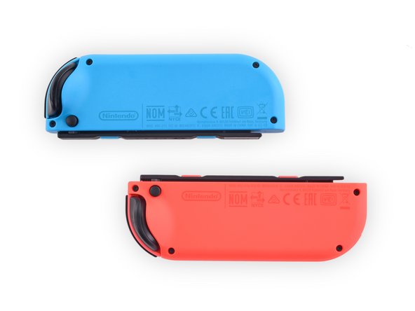
こうして見るとコントローラーの色の比較がよくできます。レッドとブルーの対決です。
-
Joy-Conはただの薄っぺらではありません。重要な中身に何があるのでしょうか。レッドの Joy-Conは IRハードウェアとNFCアンテナが搭載されています。
-
レッドとブルー、同一ものは何があるでしょうか?Joyスティックを留めている2本のプラスネジとボードに留められた2本のプラスネジ。これだけです。
-
ブルー、私たち修理士たちのために必要なときにそこにいるのですよね。
-
それぞれの基盤下部に重いHD振動モーターがあり、これは5.5gあります。
I had to send my Left Joy-Con for a repair on day one because the L button was acting erratically. I first noticed it when I tried to write my credit card number. I had made a mistake and tried to go back using tbe L button. When I pressed the button, my text cursor moved all the way to the left even though the button was in normal position (seemingly unpressed).
I wonder what caused this. Fun fact: Pressing the plastic piece between ZL and L button activated the sensor for L button.
Does the iFixit team has any idea what caused my problem? Thanks!
Any component info on the Joystick? Manufacturer ROM etc?
does some one know what could be the problem, after replacing the joy stick everythink works fine except that the switch doesn’t detect the joy con attached to it but if i conect it to it, it stills charge the joy con
-
-
-
より多くのICチップを探してコントローラー基板を並べてみました。ここには多くの注目すべきレッドの基板ボードがあります。(ブルーの基板は少し形が異なりますがほとんど同じビットです)
-
Broadcom BCM20734 Bluetooth 4.1/2.4 GHz トランシーバー
-
STMicroelectronics ST21NFCB NFC コントローラー
-
Macronix International MX25U4033E 4 Mb CMOSフラッシュ
-
STMicroelectronics STM32P411 32ビットマイクロコントローラー
-
STMicroelectronics LSM6DS3H 3軸加速度センサー/ジャイロスコープ (おそらく)
-
Texas Instruments BQ24072 パワーパスマネージメント付きリニアバッテリーチャージャー
-
Rohm BD27400GUL モノクラスD オーディオアンプ
Would love to see photos of both controller PCBs. Only one side is shown.
I would also like to have both joy-con because I had to send the Left one for a repair because I had troubles with the L button.
Is that white quad next to home button LED?
How can I buy this whole piece?
-
-
-
最新分解情報:隠れた秘密を確認するために、私たちはハプティック(触感)フィードバックモーターの上部カバーを開口しました。リニア共鳴アクチュエーター(LRA)はSwitchのHD振動を動かしています。
-
次にOculus Touchのハプティックモーターを取り出して比べてみました。すると内部もこのSwitchの内部ととても似通っています。
-
内部を見てみます。バイブレーションのモーターはとても標準的です。移動質量アセンブリに装着されているボイスコイルが両側に強力なマグネットで挟まれています。
What, no slow mo video?
If it is like this haptic module, it appears to be able to oscillate in 2 axes: http://www.alps.com/prod/info/E/HTML/Act...
-
-
-
Switch本体にメスを入れる前に、私たちの友人であるCreative Electron に観察をしてもらいました。待ち受ける罠にはまりたくなかったからです。
-
さて真面目な話です。レントゲン画像では私たちが発見していたことよりももっと面白い結果がわかりました。あらゆる意図や目的のために、ドックは多くのポートが搭載されたボックスの中で基板から成っています。
-
USB 2.0ポートー2本
-
ACアダプターポート
-
HDMIポート
-
USB 3.0ポートー1本
How much ampere are the USB ports ??
-
-
-
ドック側のチップ情報です。
-
Macronix International MX25L512E 512 Kb CMOS フラッシュ
-
Macronix International MX25V2006E2 Mb CMOS フラッシュ
-
Megachips STDP2550 Mobility DisplayPort (MyDP) to HDMIコンバーター
-
Rohm BM92T17 USB-C パワーデリバリーコントローラー
-
STMicroelectronics STM32P048 32ビット マイクロコントローラー
-
VIA Labs VL210USB 3.0 ハブコントローラー
-
Rohm BM92T55 USB-Cパワーデリバリーコントローラー
I would love it if someone could provide a drawing of the motherboard with dimensions in inches. For 3d printing purposes.
can get a name/model of the ribbon cable from the board that finishes as usb-c?
I need the same information. Have you figured it out yet?
I need another ribbon cable. What type would be a good replacement
What’s the part on the dock pcb that holds the ribbon cable (zif connector )
-
- デジタイザー以外ではネジが接着剤の代わりに使用されており、コンポーネントを固定しています。
- アナログスティック、ゲームカートリッジリーダーやヘッドホンジャックを含む多くのコンポーネントは交換可能です。
- バッテリーはケースに接着剤で留められており、モジュール式です。そしてエンドユーザーによって交換可能です。
- デジタイザーやディスプレイは修理作業半田付けされていません。そのため修理にかかる費用はかかりませんが、作業が複雑です。
- プロプライエタリのトライポイントネジが使用されているため、Switch本体が開口されるのを塞いでいます。
- ディスプレイとデジタイザーを交換する際は熱処理をして、強力な接着力が必要なため半田付けが必要です。


Consideraciones Finales
Calificación de Reparabilidad


(10 es lo más fácil de reparar)
Un agradecimiento especial a estos traductores:
96%


Estos traductores nos están ayudando a reparar el mundo! ¿Quieres contribuir?
Empezar a traducir ›

135 comentarios
So there's 4GB RAM?
Yes it has 4GB of RAM in the form of 2x 16Gb (or 2 gigabyte each) Samsung LPDDR4 RAM chips.
acaaew -
Does the HD Rumble operate the same way Apple's Taptic Engine works?
Probably not. The Taptic Engine is a linear oscillator, but the Switch probably uses a 3-D oscillator: That means the weight can move freely in all three directions.
Single pair of wires means single axis of movement.
Lemming -
two wires true, but magnets are magnetized diagonally and the W shape of the spring arms gives different spring rate in X and Y. Powered, the coil moved diagonally to the corner. Once let go, it occilates in different frequencies in X and Y.
Max Chen -
Well it's double the RAM in the Wii U. Four times as much if you count the 1 GB used by the Wii U OS when not playing games.
But also let's not compare Apples and Oranges, ARM architecture needs much less RAM than x86 to perform well, you can't simply compare ARM, PowerPC and x86 with 4GB of RAM and think they will all have the same performance.
<<<But also let's not compare Apples and Oranges, ARM architecture needs much less RAM than x86 to perform well>>>
No it doesn't. That's just...not correct at all.
And yeah, Switch has 2x the RAM as Wii U, though who knows how much will be accessible by games. Obviously all consoles reserve some RAM, but for some reason the Wii U reserved half of it (though that still left more than 2x the RAM versus 360 and PS3, which is maybe why they didn't care that they were reserving so much).
wolfpup3 -
Does the micro sd slot support UHS II (ie. has support for two rows of pins inside)? No one seems to care about this info in the teardowns lol
I care a lot myself too. I would even like to know what spec version of the SD Association it supports. Does it only comply to version 3.01 (UHS-1) or could it comply to the new 5.1 version or even 6.0?
Thank god i'm not the only one that cares about this. The difference between UHS-I and II could mean half of game load times from the microSD.
Ashler -
I too would like to know this. [and on all devices.]
Josh -
Looking at the photos, It does not have the extra pins, it only has 8 legs, common for a plain SD card reader.
Game load times always seem to be CPU bottlenecked on consoles anyway.
Possibly the most interesting part of the design.
Do we know the thermal envelope of the cpu/gpu? I'm wondering if it's on the verge of needing a fan. If so, a die shrink version might not need the fan anymore freeing up a lot of space for a bigger battery.
Added! Check out step 21.
I agree with Vince, I'd love to see what's inside that rumble pack. I'm betting on the same thing apple has with their taptic, but with a slightly heavier weight.
Modular eMMC? I smell bigger storage variant from Nintendo.. Anytime Soon..
Makes me wonder if we could clone the drive onto a larger drive.
Like the wiiU they know it's kinda a small amount but most people won't care at launch. I bet they even double it by xmas. Or make a more expensive version with the charging dock, 64 memory, and a Zelda or mario included. It will seem like a deal!
Guys any info on the antenna in the main body of the console or joycons for the broadcom chips? I cant see much of a BT antenna in the joycons at all from the pics. Unless theyre PCB etched?
The BT antenna in the blue joycon is pcb etched, just on the outside of the joystick. I don’t see it on the red joycon pcb at all, though.
sigoshi -
Can we get an x-ray of the HD rumble motor? Would be interesting to see how it works and whether it's a similar mechanism to the Taptic Engine.
Jason, I'm assuming that you are wanting a video of the LRA in action as a static X-ray of the device would look pretty much like what the teardown looks like only with less color. There's an awful lot of metal there and it's just going to look like a dark block.
Actually, if you look at the X-ray of the system with attached controllers, you can easily make out the dark blocks that are the LRAs.
Would it be theoretically possible to deliver HDMI over USB-C when you are not docked? I'm thinking when you visit a friend and you don't want to bring the dock etc. to play on a big screen.
You can disassemble the dock and bring the internal board along
Let the time work. I think there will be cables to get the HDMI out of the USB C. In the past, for every console there was a lot of non Nintendo accessories from third-party. Why should it be other this time?
There are many YouTube vids trying out different USB-C 2 HDMI docs, but AFAIK there is noone which works until now.
I tested it myself with the Microsoft Display Dock for its latest Lumias, but it did not work. Hopefully there will be a solution soon as I use my switch docked at two different locations and do not want to pack the dock everytime.
Megachips STDP2550 Mobility DisplayPort (MyDP) to HDMI Converter, part of the dock. You need a MyDP to HDMI converter, as the Switch puts out DP and not HDMI.
Theres no Nintendo word write on the board why this is not a Nintendo console?
This is a Nintendo Console.
Does anyone know what the voltage range of the AC adapter is? Is it 100-240 V AC considering the Switch is now a region free console?
It's USB-C on the console and the dock. Any USB-C charger should provide a charge - so if you had an international charger that supports USB-C you should be good. One of the photos shows 15V / 2.6A input on the dock and the same on the tablet itself.
The x-ray they show at the top shows the US-style prongs on the charger and those are sold supporting US voltage only with a built-in USB-C cable (i.e. the cable can't be unplugged and used on a different adapter)
Jimmy -
The charger that came with my US Switch is rated 100-240. Finally I can throw my transformer away.
Region free powersupply's are very common these days. They are cheap. Under 75W they are more cheaper, because in the EU you will need PFC over 75W. Active PFC is expensive, so a non region free supply will be get more benefit to the manufacturer @75W+.
So the charger of the Switch and every Phone are under 75W and can be build simply with an PSU driver chip and only a few more components. For every Voltage.
Although it is true that 100-240V power supplies are very common, previous Nintendo portables have been something of an outlier in this regard. The charger with my 3DSXL was 120 only, and that was 2012, years after 100-240 was standard elsewhere.
I wonder if the Bluetooth transceiver different in both joy con, as there are connection problems in the left one but not in the right one.
Well it would be pretty boring. It's just a 16 GB storage chip on a fiberglass board with gold-plated contacts.
Wow, 16GB cartridges? That's pretty awesome! I loved back in the day when Nintendo Power would list cartridge sizes, just because I'm curious about stuff like that...wish I knew how big a given 3DS/DS/Vita game I'm playing was.
wolfpup3 -
There's definitely 4GB of RAM inside of the Switch...two 2GB chips of LPDDR4.
Max bandwidth of the 3.0 port for the console? Could be very telling when/if Nintendo launches a dock with an upgraded GPU in it that could (possibly) run in SLI with the SoC GPU.
It would had been better if it was USB type-C 3.1 with Thunderbolt 3.0 for that purpose. Thunderbolt 3.0 is 8x faster than USB 3.0 and to act like a SLI eGPU, 5Gbps isn't enough for a considerable boost, if it was Thunderbolt 3.0 it would be much more future proof. Since it's just USB 3.0, I'm not sure if Nintendo is really thinking about an eGPU, which is a pity. But I hope someone with more knowledge could say what could Nintendo actually achieve with USB 3.0 regarding an extra graphics boost, I wonder if that would be enough for 4K in the future, but it doens't look like it.
Even TB 3 ends in PCIe 3.0 4x. This is to slow fore 4K gaming too. The actual 4K Graphics needs PCIe 3.0 8x as minimum to run with more than 24 fps.
It is no eGPU in existence that can bring a low power system 4K gaming. For the Switch die CPU will be the next limiting part.
You'll never get any form of functional dual GPU solution through USB - both bandwidth and latency are far too bad for that to be even remotely functional. Not going to happen.
And for those of you talking about Thunderbolt 3: TB3 is an Intel-developed tech. There's zero evidence of it even being considered for implementation outside of X86 systems. Heck, it doesn't even work on AMD-based systems, and those are X86! TB3 on ARM will never happen.
Thunderbolt is an Intel proprietary external PCIe port. Nvidia would need to develop their own proprietary external PCIe solution.
The Switch would also need extra hardware for this, mainly a couple more ICs.
But it could work since USB type C allows an extra set of data lanes to be used at a non-USB port, this is how the Switch outputs a MyDP signal (which the dock has a MyDP-HDMI converter). But currently, the Switch doesn't have supporting hardware for an external/hybrid gpu setup.
I don't know what its wrong with the guys befor me, but it's definitly USB 3.1 Standart with an USB-C Port.
USB-C is a standart for the port/plug, and can be provided with USB 2.0 to 3.1.
Only USB 3.1 Standart provides the feature of sending video signals over the cable, and the technical Standart USB 3.1 must be shipped with an C-Port/plug.
That make TB3 only 4 times faster, in cost of an proprietary plug and protocol.
Nintendo isn't so uneconomy and so the choice was USB, cause everybody got USB-devices.
Sounds like a really bad idea to be honest.
How do the joycons charge from the console, where are the connectors for power transfer?
Step 17 picture 3 -> metal contacts with flatflex cable tu the joycon pcb.
Also step 13, third picture, is the Switch's side of it. The contacts are on the underside of the rail.
Is digitizer is made of glass or plastic?
It is made of plastic.
So the cooling setup goes SoC - thermal paste - copper shim - thermal paste - cold plate - thermal paste -back plate. Granted the cold plate and heatpipe is the main deal, not the backplate.
You could argue that's similar to a CPU integrated heat spreader, but those are more form fitting and sometimes soldered for better heat dissipation. Cooling setup seems like a not great design, especially as DF clocked the vent area at 52 degrees Celsius. From a mobile SoC.
It's actually;
SoC > thermal paste > the shield/cover around the SoC and nearby components > copper shim > thermal paste > pad >mounting bracket and copper pipe, with what looks to be a layer of material between the bracket and heatpipe; also can't tell if the bracket is brazed to the sides of the heat pipe, or if it's under the heat pipe > thermal paste > backplate.
Also keep in mind that the SoC has an internal heat spreader, with is either soldered or pasted to the chip itself. So there's even more interfaces.
The 'pad' on the heat pipe can be seen on Gamer Nexus' video here: https://youtu.be/obz5tE1mdV0?t=10m46s
I also wonder what effects that shield/cover on the SoC is going to have on the DRAM it covers when it heats up.
So there's 10+ parts on top of the silicon including the IHS and it's solder/paste, 9 if the mounting bracket is brazed to the sides of the heat pipe, 10 if the heat pipe is on top of the bracket. Keep in mind that a standard computer only has 4-5 layers on top of the silicon.
Thanks your well-detailed analysis it's possible to complete wikipedia semantic info about objects components and get this:
https://tools.wmflabs.org/reasonator/?&q... (look at "has part" section)
P.D.: more info https://meta.wikimedia.org/wiki/WikiObje...
I'm guessing the screen cover is made of plastic and not glass?
Yes, the screen cover is made from plastic.
What about the cartridges? Can you open one?
Came here to ask this as well. Display is TN or IPS?
Definitely not TN, the viewing angles are great. But, idk if it's VA or IPS.
What are the screw dimensions? It would be nice to have a set of spare screws sitting around to replace them if they break/strip whilst opening the Switch in future.
Your teardown doesn't seem to include flavors of any of the components... Was this an oversight, or are you planning to update this information in the future?
Now let's hope that Nintendo will start replacing all the systems that shipped with dead pixels instead of telling us it's normal.
Nintendo Switch Dock Set (with a separate Switch Dock, AC adapter and HDMI cable) will cost $89.99. After seeing this video, Nintendo is really screwing over the consumer with a price like that.
No they're not, at least not versus what anyone else is charging. These types of adapters are expensive, and it's an active adapter.
Maybe they should be much cheaper, but Microsoft, Apple, etc. charge similar.
wolfpup3 -
Can you give a close up and any part number on the usb port on the switch. I would love to know if that is an off the shelf part that I could get from digikey if need be. It appears to be a midmount design that I am familiar with(Molex I think), but I cant get a clear shot of it from your pictures
You can click on any of our photos and delete the .huge from the end of the URL to view it in full/original resolution (which is usually 30+ megapixels). Here's the shot of the USB port on the Switch Console motherboard. Hope it helps you find what you are looking for!
Kinda want to try swapping thermal paste with some Arctic Silver or something to see if it improves dissipation at all. Not sure that would aid performance but might be worth a go. Not really sure how I'd measure any impact though... Can't exactly monitor the Chip temp.
Or perhaps with Coolaboratory liquid ultra. Check it out! It smokes Arctic Silver in the tests.
I was wondering if it was possible to take apart the front of the dock and get rid of the rail that could scratch the screen. Seems like it should still be functional after completely removing it.
Then you risk the Switch falling over as its vertical rather than at an angle. So you get a scratched screen AND potentially destroy the USB-C connector, the most difficult part to replace.
It looks like different Switches use different eMMC chips.
Yours had a Toshiba THGBMHG8C2LBAIL.
Gamer Nexus' Switch had a Samsung KLMBG2JENB-B041; seen here https://youtu.be/obz5tE1mdV0?t=9m40s
Samsung's is .2mm thicker at 1mm thick.
I'd like to see someone do a swap with a larger sized chip.
Update: according to a forum, the devkit switch has a 64GB chip, and people have already done mods to read and write the chip outside of the switch.
The only problem that might arise is the Samsung chip has 2bit MLC (Toshiba doesn't give that spec) on their 32GB chip in the Gamers Nexus' Switch, their largest 2bit MLC chip is 128GB, they offer a 256GB chip but that has a 3bit MLC.
There's hope for storage mods, and there's hopes for a larger storage switch.
Can anyone find out what size the player number LEDs are that are on the joycons?
As always, a great tear down iFixit! Thanks for keeping the world in the know!
Was the left Joy-Con's 4-button mechanism (circuit board & chassis) the same as the right Joy-Con's? I'm planning on modding a Joy-Con with a replacement (Sega Saturn) D-Pad, so I'd love to see more detail about the D buttons, for example, popping off the rubber buttons on the Joy-Con board and see what's underneath (something you could potentially solder to?). Thanks.
So how can I tell I will be buying a switch with the fix version of controllers that no longer loses connectivity?
Really need to find a replacement speaker as well. My right speaker started popping then now no sound comes out unless i put pressure on the membrane. Basically its broken now.
Mptp -
Update: My right speaker started popping and then just stopped working. I sucessfully replaced it with a New 3DS speaker
Mptp -
Is there anywhere I might be able to buy replacement parts for the switch?
The ZL button of my left joy-con is not responding. Does anybody knows if this is something that can be fix? Or i gonna need a replacement?
What do you use for doing X-Rays ?
Is there a place to order replacement parts? My Joystick is jacked up and needs replaced.
+1
I'm just looking for the L + XL buttons ribbon cable. Where can we get replacement parts?
Very Cool! I want to see the graphics card next time!
When does the replacement parts comes out?
Hey there, I've managed to have something jam the USB-C port and it's mushed the end of the black pin connector. How feasible is it to bring the system to a local repair shop and have them replace the port for me? Am I out of luck and will have to send it in to Nintendo for repairs?
If I tore a ribbon cable in a joy on, any ideas on where to source a replacement?
Was it a ribbon from inside your JoyCon?
Patrick Frost and John Horne were asking question about the antenna or antennas. SamitSakar wrote an article on the users complaining about the weakness of WIFI. If the wiring is incorrect which Patrick Frost alluded to then how does it get resolved. Is there only one antenna or more. For example iphone has 9 antenna. Slide 11, Researching the Broadcom/Cypress BCM4356 features “Single-stream and dual-stream IEEE 802.11ac solution with data rates up to 433.3 and 866.7 Mb/s” Hence it’s not the chip but the antenna configuration. Perhaps there should be more. Any input? All ears?
Hello our son has inserted a Micro USB into the USB-C socket. Now the pins are bent and the Device cannot be loaded. Does anyone know where I can get a Nintendo USB 3.1 Type C jack to replace it or an alternative jack?
Can anyone direct me to a place where I can find replacement MicroSD card boards?
Can someone help me? On step 19 , there’s a flex cable coming out of the joycon where the LED is , mine is malfunctioning it doesn’t work properly , if I open the joycon and stretch the cable the led lights works normally , but when I fold it to close the joycon it stops working, I think the cable somehow is broken inside I dont know…but anyway , is there a place that I can buy only this part so I can replace it? I don’t even know the name of this cable ;(
Any clues on the model of the IR camera? I’m interested to know how sensitive it is, the Labo shows some interesting stuff, but it makes me wonder if it’s got a high enough resolution to read QR codes made up of reflective material.
Hi I strip one of the screw of bad that even super glue did’t work. To remove the glue is use a drill (1mm) drill bit and hand turn to scrape the glue out. Anyother idea? Will epoxy work?
Where can I buy all of these parts featured in the video?
How many Connector Pins are on/what kind of connector is on the Swich LCD Flex Cable
I wouldn’t knock it for the tri-wing screws. They use Philips plenty once you get in. they are meant to act as a deterrent to mildly curious children who can get their hands on a small Phillips a little too easily “speaking as a former kiddo that broke a toy or two in this way…”. i’d say good job Nintendo overall and would give a slightly higher repair-ability score. maybe an 8.5.
my switch dont charging i have replace the chip M92T36 but nothing help
the switch dont starting
any Idea?
The upper shell (where the digitizer mounts) looks as if it can come off with about 8 more or so screws? I'm looking to replace this part due to cracking as well as replacing the digitizer and a few internal parts as well. Any tips?
Beefy Battery? Yeah right
Lacks sizes for the screws and generally leaves details out.
Hi Zachary, be sure you check the header at the top of this teardown! “This teardown is not a repair guide. To repair your Nintendo Switch, use our service manual.” We use teardowns as an entertaining, educational look inside a device not a step-by-step guide! Thanks for stopping by!
If the joycons started to always move forward and not let you jump in games what would need tobe fixed? just the buttons or like the whole board and for the stick wouldnt it just be the stick?
Hey Miles! That sounds an awful lot like the dreaded Joy-Con drift that’s been plaguing switch owners lately. The good news is, if you head over to http://support.nintendo.com, they’ll probably be able to get them fixed up for free! If you don’t want to ship them out to Nintendo, we can sell you the joystick by itself. I’m working on the replacement guide right now, it should be ready next week. Swapping out the joystick yourself only takes about half an hour, and should fix the issues you’re having.
Howdy, just wanted to tell people be very very careful when removing the joycon battery clip. Those things are super cheap and flimsy. I broke one, even being gentle. After some different approaches and a digital microscope I still haven’t figured out a safe reliable way to repair one. If I ever do I’ll post it.
Thanks a lot for this guide !
Danke für dieses kleine, aber ausführliche Tutorial